


Please Leave Us A Message
Privacy statement: Your privacy is very important to Us. Our company promises not to disclose your personal information to any external company with out your explicit permission.
 May 30, 2023
PCB component placement requirements.
PCB layout rules should be strictly referenced
(a), the specific requirements are as follows:
1. Orientation of component placement
A. Placement of components Consider wiring, assembly, welding, and maintenance as much as possible. Components on the PBA require as much as possible a uniform orientation, and components with positive and negative polarity must have a uniform orientation.
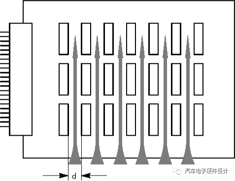
B. For the Wave soldering process, the component placement direction is shown in Figure:
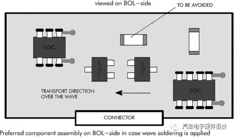
Due to the shadowing effect of Wave Soldering, the component direction is 90° to the welding direction, and the wave soldered surface element is
The height limit is 4mm.
C. For the hot air reflow process, the orientation of the components has little effect on the welding.
D. For PCBs with components on both sides, larger and denser ICs, such as QFP, BGA, etc., are packaged on the top layer of the board. The plug-in components can only be placed on the top layer, and the other side of the packaged components (bottom layer). Only small components and patch elements with fewer pins and loosely arranged components can be placed. The columnar surface mount device should be placed on the bottom layer.
E. For the structure of the vacuum fixture, the maximum height of the components on the back of the board shall not exceed 5.5mm; if a standard acupressure test fixture is used, the components on the back of the board shall not exceed 10mm.
F. Considering the actual working environment and its own heat, components should be placed in consideration of heat dissipation factors.
Note:
1. The arrangement of components should be conducive to heat dissipation. If necessary, fans and heat sinks are used. It is especially important for small-size, high-calority components and heat sinks.
2. Heat sinks can be used to dissipate heat from components such as high-power MOSFETs. Do not place heat-sensing components around these components. If the power is particularly large and the heat is particularly high, heat sinks can be added for heat dissipation.
The above is the Wave soldering process, component placement direction requirements we have listed for you. You can submit the following form to obtain more industry information we provide for you.
You can visit our website or contact us, and we will provide the latest consultation and solutions
Send Inquiry
Most Popular
lastest New
Related Products
Send Inquiry
Send Inquiry

Mr. Zhang Peter
Tel:86-0755-29098202
Fax:86-0755-29098202
Mobile Phone:+8613544118272
Email:smt@mj880.com
Address:2nd Floor, building 34, Second Industrial Zone, Shapu Wai community, Songgang Street, Bao 'an district, Shenzhen, Guangdong
Related Products List
Mobile Site

Privacy statement: Your privacy is very important to Us. Our company promises not to disclose your personal information to any external company with out your explicit permission.
Fill in more information so that we can get in touch with you faster
Privacy statement: Your privacy is very important to Us. Our company promises not to disclose your personal information to any external company with out your explicit permission.