


Please Leave Us A Message
Privacy statement: Your privacy is very important to Us. Our company promises not to disclose your personal information to any external company with out your explicit permission.
 June 12, 2023
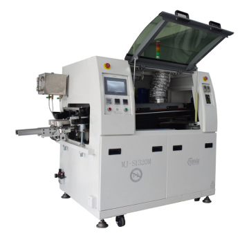
Wave soldering is to make the soldering surface of the board directly contact with high-temperature liquid tin for welding purposes. The high-temperature liquid tin maintains a slope, and the liquid tin forms a wave-like phenomenon by special means, so it is called “Wave Soldering”. The material is a solder bar. At present, the Wave Soldering Machine basically adopts the heat radiation method for preheating. The most commonly used wave soldering preheating methods include forced hot air convection, electric heating plate convection, electric heating rod heating and infrared heating.
Wave soldering procedure flow
1. Preparation before wave soldering
Check whether the PCB to be soldered (the PCB has been coated with SMD adhesive, SMC/SMD patch, adhesive curing and THC insertion process), and the soldering surface of the component socket and the gold finger are coated with solder resist or Stick with a high-temperature adhesive tape to prevent the jacks from being clogged with solder after the wave crest. If there are larger sizes of slots and holes, apply high temperature adhesive tape to prevent solder from flowing to the upper surface of the PCB during wave soldering. Connect the flux to the hose of the sprayer.
2. Open wave soldering furnace
a. Turn on the wave soldering machine and exhaust fan power.
b. Adjust the width of the wave soldering machine belt (or fixture) according to the PCB width.
3. Set wave soldering parameters
Flux flow rate: Determined based on the contact of the flux with the underside of the PCB. The flux is evenly applied to the bottom surface of the PCB. It is also possible to observe from the through holes in the PCB that a small amount of flux should penetrate upward from the through holes to the pads on the through hole faces, but do not penetrate the assembly body.
Preheating temperature: According to the actual situation of the preheating zone of the wave soldering machine (the upper surface temperature of the PCB is 90-130 °C, the upper plate, the thick plate, and the assembly board with more components have the upper limit)
Conveyor speed: set according to different wave soldering machines and PCBs to be soldered (typically 0.8-1.92m/min)
In the tin pot, the temperature of the meter or liquid crystal display is about 5-10 ° C higher than the actual temperature of the peak)
Height of the probe: Adjusted to the bottom of the PCB, 2/3 of the thickness of the PCB.
4. Wave soldering and inspection (after all welding parameters reach the set value)
a. Gently place the PCB on the conveyor belt (or fixture) and the machine automatically sprays flux, drying, preheating, wave soldering, and cooling.
b. Hold the PCB at the wave soldering exit.
c. According to the factory inspection standards.
5. Adjust the wave soldering parameters according to the welding results of the parts
6. Continuous wave soldering production
a. The method is welded to the same piece.
b. At the wave soldering exit, catch the PCB. After inspection, put the PCB into the anti-static turnover box and send it to the repair board.
c. Each printed board should be inspected for quality during continuous welding. For printed boards with severe soldering defects, the soldering should be repeated immediately. If there is still a problem after repeated welding, the cause should be checked and the process parameters adjusted accordingly before welding can be continued.
7. Inspection standards are in accordance with factory inspection standards
8, note:
a. Reflow Soldering preheating temperature heating rate does not exceed 3 ° C per second, the internal high temperature heating device is carefully burned.
b. When the furnace is over, the PCB placement distance is at least 3cm.
c. When the wave soldering temperature is unqualified, stop using it immediately. The equipment or engineer of the relevant engineering department will check and adjust the wave soldering temperature before checking. After passing the test, the computer board B can continue to be placed.
d. The technician must check the temperature settings of the wave soldering every day and make actual measurements with a thermometer. The temperature must be within the specified range.
Wave soldering technical requirements
The above-mentioned guarantee conditions only have the basis of welding. To weld high-quality printed boards, it is important to set the technical parameters and how to make these technical parameters reach the optimum value. The solder joints are not exposed to soldering, soldering, bridging, pinholes, bubbles, cracks, tinning, and sharpening. Setting parameters should be tested and analyzed, and a set of optimal parameters should be found and recorded. If similar input conditions are encountered later, the mature parameters can be set directly without having to test. Flux flow control: Set reasonable parameters through the test, the components are general through-hole devices, and the flow rate is 1.8L/H篊 tilt angle control: the tilt angle is between the horizontal surface of the peak and the printed board at the peak. The angle of the adjustment is strictly controlled at 6-10 篊.
Wave soldering furnace temperature and time control
The wave soldering dwell time is the time from the contact wavefront to the exit wavefront on a PCB. The stop/weld time is calculated as: dwell/weld time = wave width / speed. For different wave soldering machines, due to the difference in width and width of the wavefront, it is necessary to adjust the conveying speed of the printed board so that the welding time is more than 2.5 seconds, and the following relationship can be referred to. In actual production, it is often only possible to evaluate the appearance quality and the defect rate of the solder joints. It is not known how the welding strength and the electrical conductivity are, and "virtual welding" comes from this. According to Qi Cheng and Che Zhaohua's "SMT wave soldering process research", during the welding process, the metallographic structure of the solder joint has undergone the following three stages of changes:
(1) The alloy layer is not completely formed, only a semi-adhesive bond, the strength is very low, and the conductivity is poor;
(2) The alloy layer is completely formed, the solder joint strength is high, and the electrical conductivity is good;
The above is the Wave soldering operation process and basic process of welding we have listed for you. You can submit the following form to obtain more industry information we provide for you.
You can visit our website or contact us, and we will provide the latest consultation and solutions
Send Inquiry
Most Popular
lastest New
Related Products
Send Inquiry
Send Inquiry

Mr. Zhang Peter
Tel:86-0755-29098202
Fax:86-0755-29098202
Mobile Phone:+8613544118272
Email:smt@mj880.com
Address:2nd Floor, building 34, Second Industrial Zone, Shapu Wai community, Songgang Street, Bao 'an district, Shenzhen, Guangdong
Related Products List
Mobile Site

Privacy statement: Your privacy is very important to Us. Our company promises not to disclose your personal information to any external company with out your explicit permission.
Fill in more information so that we can get in touch with you faster
Privacy statement: Your privacy is very important to Us. Our company promises not to disclose your personal information to any external company with out your explicit permission.